The development trend of power inductors:
1. Fine power inductor
The biggest challenge in the design of power supplies for portable electronic products is to improve the efficiency of the power supply while reducing its size, which means it is best to use the smallest inductor in power supply design.
The lower inductance value caused by load fluctuations in transient response is better offset. In this case, with the faster transient response caused by load fluctuations, the low inductance value shifts due to high frequency.
However, there are gains and losses, and increasing the switching frequency also increases the switching loss, which can also lead to a decrease in work efficiency. Due to the fact that the interaction between other important circuit designs can affect device performance, simply increasing the switching frequency is not an easy task.
However, further refinement of the internal circuit has resulted in a switching frequency of up to 3MHz, while the inductance value is also below 2.0H. According to calculations, switching frequencies of 6-8MHz and inductance values below 1H are not common, which leads to the dramatic miniaturization of inductors.
2. Higher switching frequency
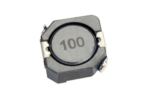
Power inductance
The development trend of Class 1-A inductors is towards small packaging, low inductance, and faster switching frequency. For example, inductors with a switching frequency of 300kHz but an area of only 16 or 36mm2 will be widely used. Using a 9mm2 inductor can increase the switching frequency to 1.5MHz, indicating that increasing the switching frequency also reduces the size accordingly. The key to providing more refined inductors in the future lies in whether component manufacturers have the ability to reduce inductance and increase switching frequency through continuous progress in circuit design, materials, and manufacturing.
The progress of inductor technology for mobile phones has been demonstrated in terms of packaging thickness, for example, from 2mm to 1mm. The significant improvement of this technology continues to attract the global electronic product consumer market with the trend of miniaturization relying on ultra-thin components to support devices. Even so, relying solely on the use of smaller inductors is not a comprehensive solution.
3. Winding improvement
Smaller portable devices require more compact and efficient DC/DC converters, relying on the powerful functions of these complementary devices to maximize battery energy. Although it is difficult for large components to simultaneously reduce inductance size and maintain low impedance, manufacturers are still reducing inductor size through better design, improved material science, and improved manufacturing technology.


 中文
中文 Follow Us
 0758-6553301
 E-mail